 AHI Journal
台積電A14 節點超前試產驅動設備升級TSMC A14 Pilot Run Ahead of Schedule Sparks Equipment Upgrades
新竹寶山Fab20 廠排定 2027 年第 1 季啟動A14 試產,耗材研磨與量測設備需求迎來新一輪擴展。TSMC slated its Baoshan Fab 20 in Hsinchu to launch A14 pilot production in the first quarter of 2027, unlocking a fresh expansion cycle for chemical mechanical planarization consumables and metrology tools.
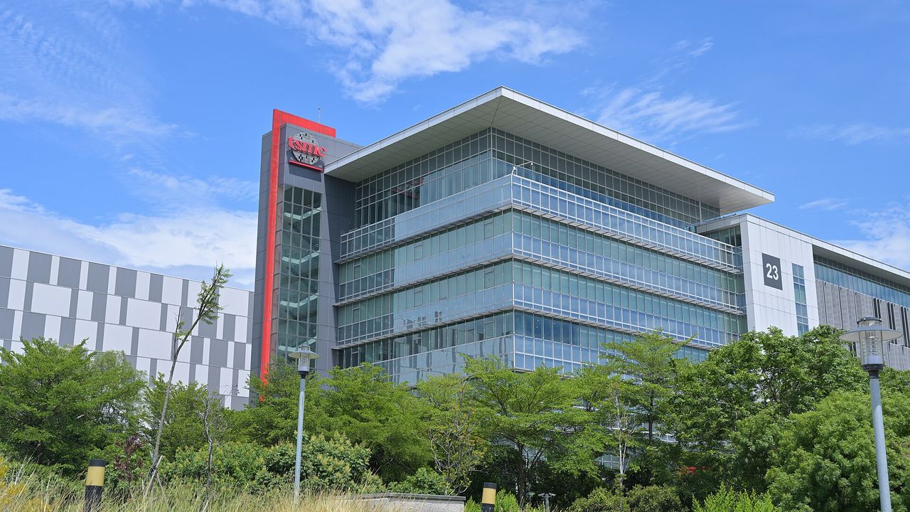
台積電先進製程推進再傳超前訊號,新竹寶山Fab 20 預計在 2027 年第 1 季啟動A14 節點試產,初期規劃月產能達 50 至 55K片。市場原先擔憂 2 奈米良率爬坡可能拖慢後續研發節奏,但AI算力軍備競賽的白熱化,迫使晶圓代工龍頭加快下一代晶片架構的佈局步調。2026 年預估高達 600 億至 640 億美元的資本支出規模中,有 7 至 8 成重押先進製程,確立了半導體設備與量測耗材供應鏈長達數年的高成長循環。這不僅是晶圓微縮技術的關鍵進展,更揭示出高階半導體產業鏈正進入新一輪硬體升級週期。TSMC is signaling accelerated progress across its leading-edge roadmaps, with Fab 20 in Baoshan, Hsinchu slated to launch pilot production for the A14 node in the first quarter of 2027 at an initial monthly capacity of 50,000 to 55,000 wafers. While markets had feared that the 2nm yield ramp might delay subsequent development cycles, the intensifying AI compute race has prompted the foundry giant to fast-track its next-generation architecture. Of its projected 2026 capital expenditure of $60 billion to $64 billion, roughly 70% to 80% is earmarked for advanced processes, cementing a multi-year growth cycle for semiconductor equipment and metrology suppliers. This milestone not only highlights progress in silicon scaling, but also confirms the high-end supply chain is entering a fresh hardware upgrade wave.
產能疊加打破節奏放緩預期Concurrent Capacity Expansions Dispel Slowdown Fears
先進節點的推進展現出罕見的重疊擴張態勢。台積電並未因為跨入埃米世代而減緩前代產能佈局,N3 製程月產能預計在 2026 年推升至 180K片以上,隔年再額外增加 40 至 50K片;而 2026 年底N2 產能更上看 140K片以上,大幅超越市場原先預估的水準。A14 初期 50 至 55K片的試產規劃在此時加入,反映出各大雲端服務巨頭對先進算力的剛性需求。多個世代製程同步擴張,意味著資本支出不是階段性的資源轉移,而是基底全面的向上墊高,消除了市場對技術節點轉換期產能斷檔的疑慮。Advanced node rollouts are demonstrating rare, overlapping expansion momentum. TSMC has not curtailed trailing capacity investments as it steps into the Angstrom era: monthly N3 capacity is slated to exceed 180,000 wafers in 2026, with an additional 40,000 to 50,000 wafers planned for 2027; meanwhile, year-end 2026 N2 capacity is tracking above 140,000 wafers per month, handily beating prior market estimates. Factoring in A14's initial 50,000 to 55,000-wafer pilot runs highlights cloud hyperscalers' non-negotiable demand for advanced computing power. Expanding multiple process generations simultaneously indicates that capex is not shifting cyclically, but rather resetting to structurally higher baselines, easing fears of an interim capacity gap between node transitions.
製程道數激增推動耗材量測升級Surging Process Complexity Drives Metrology and Consumables Upgrades
隨著晶片結構向更微小節點演進,物理極限的突破直接轉化為製程工序的倍數增長。A14 全製程的化學機械研磨工序已大幅攀升至 60 至 70 道,相比前代架構的用量增長超過 3 成。工序密度的跳升帶來晶圓表面平整度與缺陷控制的嚴苛標準,連帶引爆前段檢測機台與關鍵耗材的升級需求。本土設備供應商在此波升級中陸續打入晶圓代工核心站點,半導體檢測設備的拉貨動能轉強,使供應鏈在先進製程資本支出的轉化過程中,直接取得技術迭代所釋放出的實質訂單紅利。As architectures push toward smaller nodes, physical scaling limits are directly translating into a manifold increase in process steps. Full-flow chemical mechanical planarization (CMP) steps for A14 have jumped to between 60 and 70 passes, representing more than a 30% increase in consumption over predecessor nodes. This surge in process density imposes stringent requirements on wafer surface planarity and defect density, driving upgrades in front-end metrology tools and critical consumables. Domestic Taiwanese equipment vendors are progressively penetrating critical foundry bays, capturing accelerating demand for metrology systems and securing tangible order momentum as advanced-node capex converts into supply-chain revenues.
機台交期與高額折舊成推進變數Tool Lead Times and Depreciation Pose Operational Headwinds
儘管技術路徑與資本投放藍圖清晰,實體交付環節仍面臨外部供應鏈的實質考驗。全球雲端大廠同步啟動客製化處理器開發,推升對極紫外光等高階曝光設備的爭奪,機台零組件交期若受地緣或供應鏈瓶頸干擾,無塵室工程與機台到位速度便可能出現落差。同時,先進節點所需投入的巨額研發與設備投資,將在啟用初期帶來顯著的折舊負擔,對代工廠的毛利結構形成實質壓力。如何在激進擴產與維持獲利體質之間取得平衡,成為新世代節點量產前夕不可忽視的營運課題。While technological roadmaps and capex commitments are clear, physical deployment faces supply-chain execution risks. Cloud majors are developing custom in-house processors simultaneously, intensifying competition for high-end exposure equipment, including Extreme Ultraviolet (EUV) systems; any component delays tied to geopolitical or supply friction could disrupt cleanroom construction and installation schedules. Furthermore, the massive R&D outlays and capital expenditures tied to next-generation nodes will generate substantial depreciation loads in the early operating phase, creating near-term margin pressure for the foundry. Balancing aggressive capacity expansion against gross-margin health remains a critical operational challenge ahead of volume production.
本刊判斷,先進製程提早試產確立了半導體資本支出上升週期的持續性。後續觀察重點在於晶圓代工龍頭對年度資本支出指引的調整方向,是否維持先進製程的高比重配置;同時須追蹤新竹寶山廠區高階機台的實際進駐時程,以此評估新節點推進是否維持超前節奏。We view this accelerated pilot production schedule as confirmation that the semiconductor capex upcycle remains intact. The key signposts to watch include adjustments to the foundry giant's annual capex guidance—specifically whether it preserves high allocations to advanced nodes—alongside delivery timelines for high-end tools at the Baoshan site in Hsinchu, which will determine whether the accelerated node rollout remains on track.
訂閱版提供各世代產能爬坡預估表、本土設備供應鏈受惠清單,與資本支出覆核條件。The subscriber edition features node-by-node wafer ramp projections, a domestic equipment beneficiary scorecard, and proprietary capital expenditure audit criteria.