 AHI Journal
探針卡版圖位移與算力治理重估Probe-Card Market Realigns as AI Governance Spurs Valuation Reckoning
旺矽獨攬輝達關鍵晶片測試訂單確立獲利躍升,然而前沿模型安全放緩言論重擊半導體評價MPI secures an exclusive testing contract for Nvidia's critical processor, boosting earnings visibility, as calls to slow frontier model development hammer chip valuations.
半導體測試介面在 9 月中旬出現重大版圖位移。台系同業因品質瑕疵退出供應鏈,使旺矽順利獨攬輝達關鍵處理器專案的原有份額,同時卡位次世代網路晶片市場。然而,硬體端的捷報未能平撫市場焦慮,主要人工智慧業者公開呼籲放緩前沿模型推進節奏以落實安全治理,隨即引發資本支出恐慌,費城半導體指數單日重挫 5.86%,加權指數亦跌破 46,000 點整數關卡。當前市場的核心爭點在於:模型訓練節奏的策略性調整,究竟是AI基建擴張週期的實質降溫,還是資金與硬體需求在結構移轉前的短期定價錯位。The semiconductor test interface sector witnessed a major reshuffling in mid-September. A quality stumble by a local peer forced its exit from the supply chain, clearing the way for MPI Corp. to capture the entirety of an order for a crucial Nvidia processor project while staking out ground in next-generation networking silicon. Hardware triumphs, however, did little to soothe market nerves. Public calls by leading artificial intelligence developers to slow the deployment of frontier models to bolster safety governance quickly triggered fears over capital expenditures. The Philadelphia Semiconductor Index plunged 5.86% in a single session, and Taiwan's Taiex broke below the key 46,000-point threshold. The central debate gripping the market now is whether this strategic recalibration in model training represents a genuine downshift in the AI infrastructure buildout, or merely a transient mispricing before capital and hardware demand pivot into new structures.
埃米製程拉高良率門檻推升耗材價值Angstrom Nodes Tighten Yield Tolerances, Lifting Consumable Value
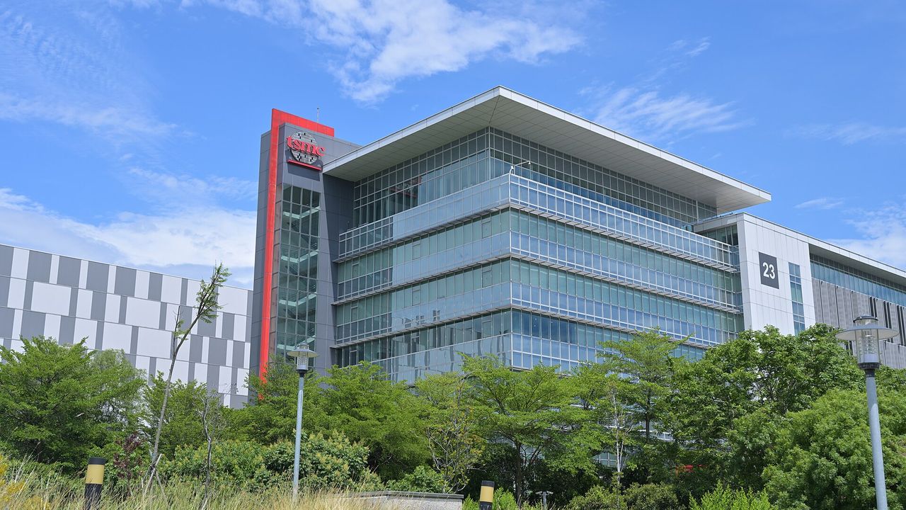
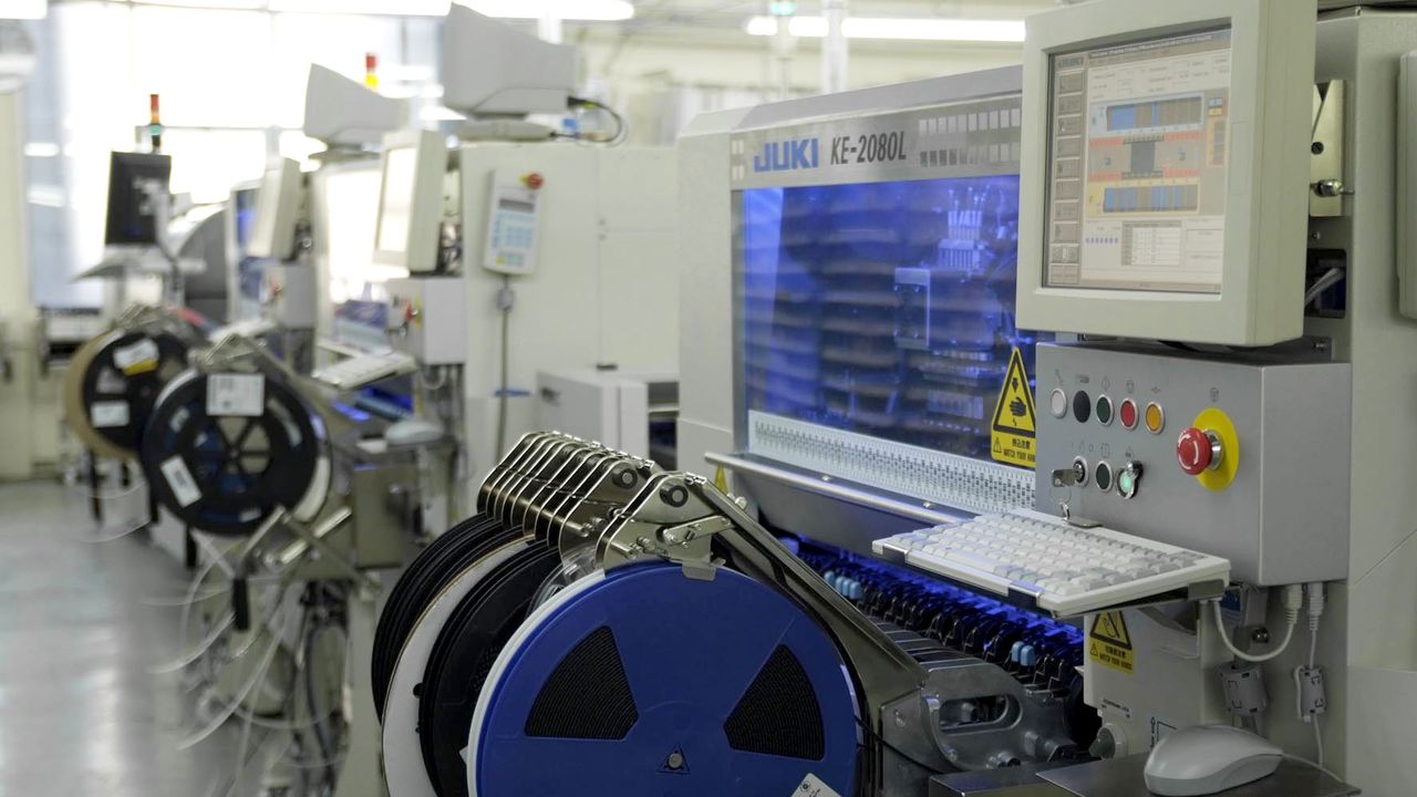
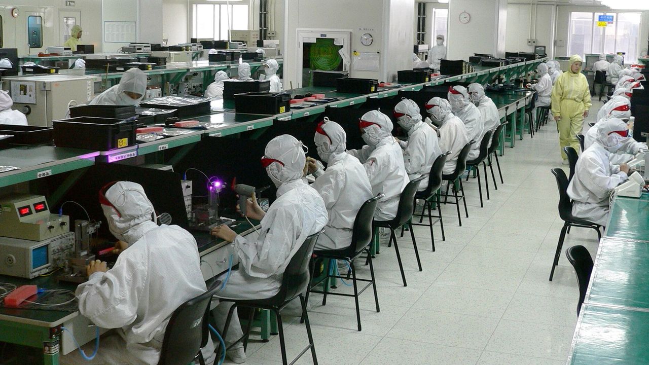
先進製程進入埃米世代與大型晶圓級封裝後,測試零組件的容錯空間已被極限壓縮。在輝達Vera CPU專案中,原本由同業掌握的 7 成訂單因品質遭遇瓶頸而全數退場,旺矽順勢由原先的 3 成配額擴張至全面獨攬。此一轉折不僅大幅推升了其獲利預期下限,更為次世代網路通訊晶片測試奠定壟斷優勢。隨著台積電三奈米與二奈米先進製程產能預計於 2026 年與 2027 年分別達到每月 7 萬片與 15 萬片規模,高階垂直探針卡等耗損零組件的消耗頻率呈幾何級數放大,晶圓測試環節正從邊緣配套轉化為晶片出貨的決定性防線。As advanced fabrication moves into angstrom geometries alongside massive wafer-level packaging, margins of error for testing hardware have been squeezed to the limit. In Nvidia's Vera CPU project, a peer that previously held 70% of the business exited entirely after hitting yield and quality bottlenecks, allowing MPI to expand its previous 30% allocation into outright exclusivity. The shift meaningfully raises MPI's earnings floor and establishes a dominant foothold in testing next-generation networking chips. With TSMC's 3nm and 2nm capacities projected to scale to 70,000 and 150,000 wafers per month in 2026 and 2027, respectively, burn rates for high-end vertical probe cards are rising exponentially. Wafer testing is thus transforming from a peripheral operational step into a decisive gatekeeper for chip shipments.
雲端巨頭營運數據證實算力轉向推論Cloud Giants' Operational Data Confirms Compute Pivot Toward Inference
軟體業者放緩模型訓練速度的表態引發了產能過剩的疑慮,但雲端巨頭的資本運作呈現不同面貌。甲骨文最新公布的雲端基礎架構營收年增 121%,在手未交付訂單高達 6,640 億美元,其部署的 30 餘萬顆運算晶片使用率維持在 97.9%高檔;Google自研晶片的投資回收期亦壓縮至 1 年之內。這些數據表明,算力需求並未減退,而是經歷結構性位移。產業焦點正由盲目衝刺基礎模型參數,轉向高頻率的商業推論應用與安全防護檢測,硬體資本支出整體規模依然穩固,只是算力架構正從單純訓練向推論節點移轉。While software developers' calls to temper training cadences sparked fears of impending overcapacity, capital deployment among cloud hyperscalers paints a markedly different picture. Oracle's latest results showed cloud infrastructure revenue surging 121% year-over-year against a remaining performance obligation backlog of $664 billion, with its fleet of over 300,000 compute accelerators sustaining a high 97.9% utilization rate. Google, meanwhile, has compressed the payback period on its custom silicon to within one year. Such figures show that appetite for compute has not waned, but has undergone a structural rotation. The industry's center of gravity is shifting from unbridled foundation-model parameter scaling toward high-frequency commercial inference workloads and security evaluations. Overall hardware capital outlays remain resilient, even as architecture pivots from raw training toward inference clusters.
功耗極限倒逼全套物理架構加速升級Thermal Thresholds Force Full-Stack Physical Infrastructure Upgrades
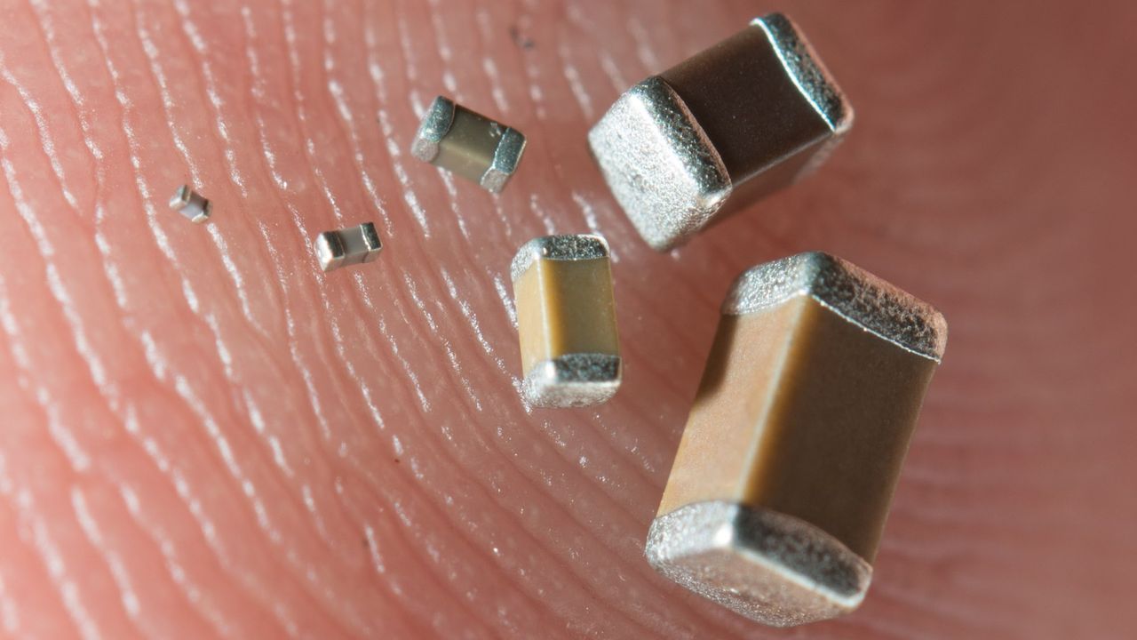
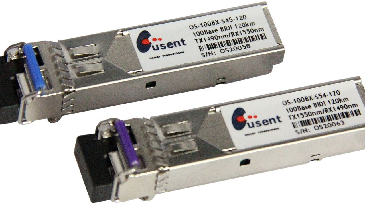
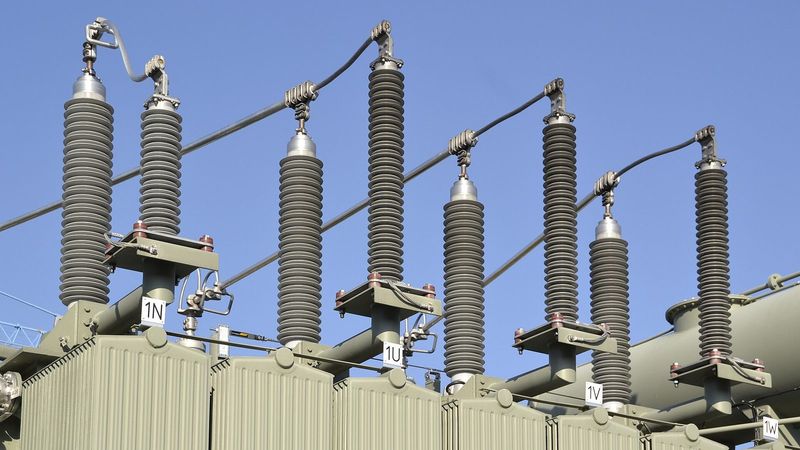
運算核心之外的物理限制,正在促使整套伺服器基礎設施展開強制升級。次世代晶片熱設計功耗正式跨越千瓦級門檻,推動伺服器液冷散熱滲透率從 2025 年的 33%快速拉升至 2026 年的 53%,並朝 2027 年的 60%推進。與此同時,電力傳輸系統全面走向 800V高壓直流架構,直接驅動高壓被動元件與功率半導體的單機價值倍數成長。整場算力擴張的實體瓶頸,已從單一處理器運算性能,延伸至極限散熱、高壓電力分配、光互連傳輸與晶圓量產測試等全套物理系統,供應鏈壁壘亦隨之深化。Beyond compute silicon, physical limits are compelling a mandatory overhaul across server infrastructure. Next-generation processor thermal design power has breached the kilowatt threshold, driving liquid cooling adoption in servers from 33% in 2025 to 53% in 2026, on track to reach 60% by 2027. Concurrently, power delivery is pivoting toward 800V high-voltage direct-current architectures, multiplying the per-rack content value of high-voltage passives and power semiconductors. The physical bottlenecks to compute expansion have expanded beyond raw processing throughput to encompass extreme heat dissipation, high-voltage power distribution, optical interconnects, and high-volume wafer testing—deepening supply chain moats along the way.
本刊判斷,短期因模型安全言論引發的半導體估值修正,並未扭轉硬體升級的底層物理邏輯。市場當前的劇烈震盪,實質上反映出資金對單純訓練擴張故事的降溫。後續觀察重心應聚焦於晶圓代工龍頭對先進製程資本支出的最新定調、高頻寬記憶體的價格議價動能,以及矽光子等新世代互連技術在量產端的實際驗證節奏。In our view, the short-term valuation reset across semiconductor equities triggered by AI safety discourse does not negate the foundational physical imperatives driving hardware upgrades. The current market volatility reflects cooling investor enthusiasm for one-dimensional training narratives. The critical signposts ahead include foundry bellwethers' updated commentary on advanced-node capital spending, pricing power in high-bandwidth memory, and the commercial qualification milestones of next-generation interconnect architectures like silicon photonics.
訂閱版提供台積電資本支出檢查點、CPO機台驗證進度門檻,以及旺矽獲利下修的關鍵否證條件序列拆解。The subscriber edition details TSMC capex checkpoint thresholds, CPO equipment verification milestones, and a sequential falsification framework for potential MPI earnings downgrades.